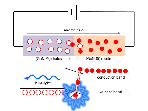
GaN is a wide gap semiconductor that is a crucial component of blue light emitting diodes (LEDs), which are essential for solid state lighting. Both n- and p-type layers are required for LEDs, but achieving p-type GaN is very difficult; the only successful method is to very heavily dope GaN with Mg. Why no other dopants result in significant hole concentrations is not well understood. Moreover, there are many photoluminescence peaks observed from a broad range of differently prepared GaN samples whose origin is a major source of debate. Using the Chemshell code to perform hybrid QM/MM embedded cluster calculations, we have shown that Mg on a Ga site cannot act as a shallow acceptor in GaN and that holes are thermodynamically unstable, indicating that defect complexes and non-equilibrium processes dominate in p-type GaN. We have developed a new methodology to model shallow donors in GaN and have carried out a comprehensive analysis of native point defects in the material, indicating which defects could be the origin of the observed photoluminescence peaks. Our results have clarified the source of many experimental observations and have stimulated debate within the community on the defect properties of this important wide gap material.
J. Buckeridge et al., “Determination of the Nitrogen Vacancy as a Shallow Compensating Center in GaN Doped with Divalent Metals“, Phys. Rev. Lett., 2015, 114, 016405.
Z. Xie et al., “Demonstration of the donor characteristics of Si and O defects in GaN using hybrid QM/MM“, Phys. Status Solidi A, 2017, 214, 1600445.
Z. Xie et al., “Prediction of multiband luminescence due to the gallium vacancy–oxygen defect complex in GaN“, Appl. Phys. Lett., 2018, 112, 262104.
Z. Xie et al., “Donor and acceptor characteristics of native point defects in GaN“, J. Phys. D: Appl. Phys., 2019, 52, 335104.